Octric
Compound semiconductor innovation for the most demanding, high-performance applications.
Our Scholarships
Placement Location
Newton Aycliffe, Co Durham
Type of Placements Offered
• Summer placements only
Restrictions/Notes
(1) Open only to British citizens (no dual nationals); (2) Candidates may be required to undergo security clearance; (3) Requires interested in Semiconductor Engineering/Technology
Who we are and what we do

Octric is the leading UK manufacturer of advanced compound semiconductors enabling the most demanding, high-performance applications including telecommunications, space, aerospace and defence.
Our semiconductor process capabilities include Gallium Arsenide (GaAs), Gallium Nitride (GaN) and Indium Phosphide (InP), and our manufacturing expertise and process innovation spanning over 25 years has delivered cumulative device shipments exceeding 1.5 billion units. With a highly talented and skilled workforce of technologists and engineers, and backed by significant UK Government investment, Octric is a trusted partner empowering global customers to deliver differentiated products to market
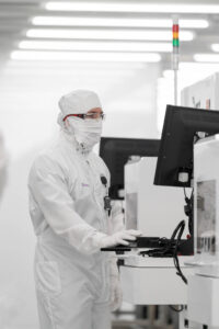
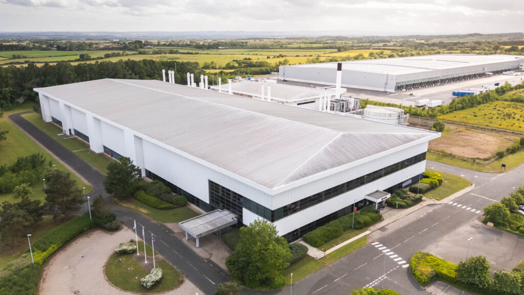
We’re developing next-generation semiconductor platforms at our purpose-built facility in County Durham, which includes a 4,800m² Class 100 clean room, one of the largest of its kind in Europe.
What you could be doing
As an intern at Octric you can expect to be part of an engineering team working on programmes that directly impact our business.
You will be assigned a project that will last for the period of your internship with dedicated support from one of our experienced engineers. The project will be defined to maximise your exposure to one of our engineering disciplines, to provide valuable experience in a high technology industry and also to ensure that your work brings real benefit to the company. Potential areas of focus can be optimised for the skills and interests of the applicant, but could include activities such as:
- Device engineering – working on our labs on wafer probe measurements of active and passive semiconductor device structures leading to data and model generation for our new technology developments.
- Process engineering – working in the fab on experiments to optimise equipment and process recipes for our new semiconductor technology developments.
- Reliability and failure analysis – working with state-of-the-art scanning electron microscope equipment to provide imaging of device failures and helping to determine root cause of failure.
- CAD engineering – designing and laying out passive and active structures to assist the modelling and failure analysis teams, coding design kits for our customers to use to design their circuits, assisting with customer tape-outs.