EDA Solutions
We support European IC design companies create silicon chips for AI-IoT, ADAS, sensor fusion and many other applications which shape today’s world. EDA Solutions
Our Scholarships
Placement Location
Fareham (Hampshire)
Type of Placements Offered
• 12-month placements only
Restrictions/Notes
(1) Requires 12-month placement for 2026/27; (2) Students must be in the penultimate year of their degree
Who we are and what we do
EDA Solutions is the European business partner for IC design solutions from Siemens EDA which means we sell and support their software products.
Founded in 2001 the company provides Europe wide sales and hands-on technical support for leading software design solutions for custom IC, MEMS and silicon photonics engineers.
We pride ourselves on our industry and technical experience with a small, friendly team of engineers based in UK, France, Germany and Israel. Our technical team provides front line support to hundreds of happy customers designing silicon chips.
What you could be doing during your work placement
 You will work with our European customers and the technical teams at both semiconductor foundries and our partner, Siemens EDA. You will undergo a structured learning program and develop technical skills related to IC chip design and people skills such as building lasting relationships, teamwork and active listening. Most importantly, from day one, you have real-work responsibilities and be actively contributing to the business.
Twelve months later you will be able to demonstrate exposure to every aspect of a semiconductor design business with design experience, new technical and people skills and workplace achievements. You will be energised for your final year of university and be very well qualified to finding your first job after graduation.
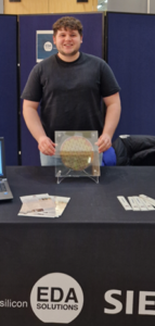
Meet one of our Scholars
Name: Ethan
Sponsor: EDA Solutions
University: University of Birmingham
Degree Course: MEng Electronic Engineering
Why I chose EDA Solutions
I chose EDA Solutions as they offered a range of experience, from software support to consultancy projects, and internal IT management. It was apparent from the job description that the skills I would gain would be invaluable in aiding me in the final year of my degree and securing future employment once I graduate. I could see the benefits of working in a small team and being given true responsibilities.
Why did you want a scholarship with EDA Solutions?
I was interested to learn more about the Semiconductor industry and the software used to design and manufacture chips. I also chose EDA Solutions for my sponsoring company as I wanted to work in a small team and learn about the whole flow from setting up machines, licensing, installation and troubleshooting the whole design flow.
What type of work have you been involved with during your placement?
The type of work I did was varied. My main responsibility was post-sale support, helping customers who have found issues with the software get sorted as soon as possible.
I also worked on a consultancy project where I helped create a co-simulator tool for mixed electrical and optical signals. I got the opportunity to learn from our partners about the photonics industry and presented the early findings at a conference in Germany.
Some of my smaller responsibilities were managing and improving the IT infrastructure, making sure the office and remote workers were online and connected and there were Virtual Machines setup for testing. I also took on some automation projects putting my coding skills to the test. I created applications writing in Python, Bash and TCL.
I got the chance to attend a Siemens EDA code-bash event where I tested the upcoming release of software and received training on the new features.
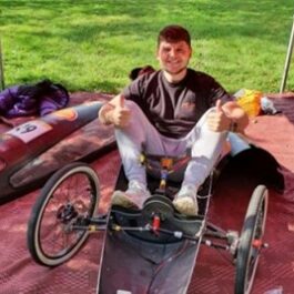
What are your hobbies and interests?
In my spare time I play handball. I was fortunate to find a local team (Vulcans) who I trained with for the year. I will be returning to my university team as I return to Birmingham. I also help build a prototype ultra-mileage vehicle to race in the shell eco marathon. We are currently in the process of switching to an electric powertrain.